


Time to read: 8 min
Building semiconductor systems is a massive engineering challenge. While many people’s first thought when they hear “semiconductor” may be tiny circuits on a chip, none of those chips could be made without the physical hardware that fabricates them—from robots, inspection machines, and fixtures to custom parts and enclosures.
In this article, we’ll explain the best ways to manufacture semiconductor equipment through techniques like CNC machining, sheet metal fabrication, and injection molding.
Manufacturing for Semiconductor Equipment Systems

What is Semiconductor Equipment Manufacturing?
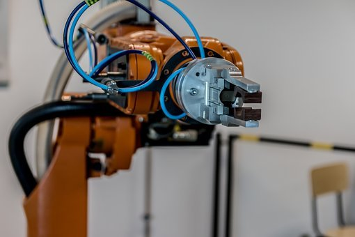
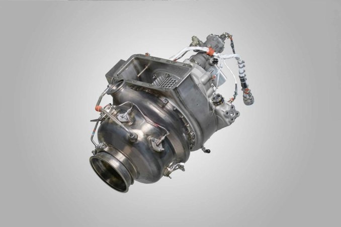
Semiconductor equipment manufacturing is the production of precision hardware systems used to fabricate, inspect, test, and handle semiconductor devices. For mechanical engineers, the focus is not on the chips themselves, but on the hardware that enables chip production. This includes wafer-handling systems, test fixtures, robotic assemblies, precision-machined components, cleanroom enclosures, and automation hardware.
Modern semiconductor systems are rarely built using a single manufacturing process. They rely on a combination of multiple disciplines to meet rigorous performance standards:
- Precision-Machined Parts: The core of wafer alignment and motion control.
- Sheet Metal Structures: The frames, enclosures, and racks that protect sensitive electronics and protect against contamination.
- Molded Components: Used for specialized housings and high-volume insulators.
- Off-the-Shelf Hardware: Standardized components that ensure speed and reliability.
Semiconductor systems demand extreme precision (often with tolerances measured in microns) and repeatability. Contamination control requires equal attention; even a microscopic particle can ruin a production batch, making material selection and surface finish critical.
System-Level Manufacturing Decisions in Semiconductor Equipment
Semiconductor equipment manufacturing is fundamentally a systems-engineering challenge. Unlike standalone industrial components, semiconductor hardware operates within tightly integrated assemblies where precision, thermal stability, cleanliness, motion control, and repeatability all influence overall system performance.
As a result, manufacturing decisions cannot be made at the individual-part level alone.
Precision Requirements Across the System
Not every component within a semiconductor platform requires the same level of manufacturing precision. Wafer-handling systems, alignment stages, and test interfaces often require micron-level tolerances, highly controlled flatness, and repeatable assembly conditions. Small deviations in geometry or vibration behavior can affect wafer positioning and downstream process performance.
Structural frames, external enclosures, cable-management systems, and support brackets, on the other hand, can often use lower-cost manufacturing methods or more standardized components without negatively affecting overall system performance. The engineering challenge is knowing where extreme precision is required, and where cost and scalability can be optimized.
Thermal Stability and Mechanical Integration
Thermal behavior is another system-level consideration in semiconductor hardware. Even small amounts of thermal expansion can introduce positional variation into motion systems, optical assemblies, or wafer-handling equipment.
As a result, material selection, structural stiffness, assembly strategy, and manufacturing tolerances should all be evaluated together. Engineering teams must consider not only how individual parts perform, but how complete assemblies behave under real operating conditions.
Key Manufacturing Processes for Semiconductor Equipment
Semiconductor equipment manufacturing relies on a variety of processes to support fabrication and assembly, from CNC machining to sheet metal fabrication and injection molding. Engineering teams must balance precision, cleanliness, thermal performance, scalability, and cost across multiple manufacturing methods simultaneously.
Below are some of the key manufacturing processes for semiconductor equipment.
Precision CNC Machining for Semiconductor Components
CNC machining is the backbone of semiconductor equipment manufacturing, primarily used for wafer handling components, alignment-critical parts, and complex fixture interfaces. These parts must often maintain tight tolerances on flatness, parallelism, and positional accuracy to ensure a perfect mechanical interface with the silicon wafer.
Surface finish requirements are equally demanding. Rough surfaces can trap particles or outgas under vacuum, which leads to contamination. Common materials used when CNC machining semiconductor components include:
- Aluminum (6061, 7075): Lightweight and highly machinable, often anodized for durability.
- Stainless Steel (316L, 304): Preferred for high-purity environments and corrosion resistance.
- High-Performance Plastics (PEEK, Ultem): Used when electrical insulation or high thermal resistance is required without the weight of metal.
Semiconductor Test Fixtures and Burn-In Hardware
Semiconductor test fixtures have some of the tightest precision requirements in semiconductor equipment manufacturing. During Automated Test Equipment (ATE) validation and burn-in testing, fixtures must create highly repeatable mechanical and electrical interfaces between semiconductor devices and test systems while maintaining reliability across thousands of test cycles.
ATE fixtures commonly use dense arrays of pogo pins, precision alignment features, and tightly controlled tolerances to create reliable electrical contact before devices move into production. Even minor alignment deviations can cause bad connections or inaccurate test results, so test sockets, alignment plates, support structures, and shielding components are typically machined to tight tolerances.
Burn-in testing adds more thermal and material challenges. Fixtures must maintain dimensional stability and perform well under elevated temperatures and prolonged electrical loading. As a result, engineers often rely on high-performance plastics, anodized aluminum, stainless steel, thermally stable composites, and specialized insulating materials.
Many semiconductor test fixtures combine multiple manufacturing processes within a single assembly, integrating machined components with molded insulators, sheet metal shielding, elastomeric contacts, and off-the-shelf hardware. Maintaining micron-level positional accuracy while controlling tolerance stack-up and minimizing particle generation requires careful coordination across manufacturing and assembly workflows.

Sheet Metal Fabrication for Equipment Frames and Enclosures
Large-scale semiconductor systems must account for thermal expansion—a frame that warps under heat can throw off the alignment of the precision components within it, for example. In many cases, sheet metal enclosures shield against electromagnetic and radio-frequency interference (EMI/RFI). Precision bending and specialized welding techniques eliminate gaps in shielding integrity while protecting sensitive logic components from external interference.
Injection Molding for Semiconductor Housings and Insulators
For nonstructural components, injection molding enables complex features like internal cable routing and electrical isolation to be built into a single part. While upfront tooling costs are higher, the ability to produce high volumes of consistent, lightweight insulating components makes it an ideal choice for the mass-production phase of semiconductor hardware.
When designing molds for semiconductor components, engineers must consider the “cleanliness” of the resin. Certain additives or mold release agents can cause outgassing issues later in the product’s life, which creates contamination risk in cleanroom and vacuum environments.
Design for Manufacturability in Semiconductor Equipment
Design for Manufacturability (DFM) in semiconductor equipment manufacturing helps ensure successful, consistent design, manufacturing, and performance of products. Key considerations include:
- Tolerance Stack-up Analysis: Ensuring that the accumulation of minor variations across an assembly doesn’t lead to functional failure in the final alignment.
- Alignment Features: Incorporating dowel pins or keyed interfaces to ensure parts can be assembled and serviced repeatably.
- Modularity: Designing systems as discrete modules that can be manufactured, tested, and swapped independently.
- Service Access: Ensuring that technicians can reach critical internal components without disassembling the entire machine, which is vital for uptime in a high-stakes fab environment.
Cleanroom and Material Considerations
A major differentiator in semiconductor equipment manufacturing is the requirement for cleanroom-manufactured parts. Common practices used to reduce the risk of contamination in this type of environment include:
- Anodizing & Passivation: Crucial for preventing corrosion and reducing surface reactivity in aluminum or steel.
- Ultrasonic Cleaning: A standard process to ensure parts are free of oils, shop dust, and machining coolants.
- Specialized Packaging: Parts must be vacuum-sealed or double-bagged to maintain purity during transit.
- Outgassing Control: Materials used in semiconductor equipment must exhibit low outgassing characteristics to prevent volatile compounds from contaminating wafers, optics, or vacuum environments.
- Particle Contamination Reduction: Manufacturing processes and surface treatments must minimize particle generation, as even microscopic contamination can negatively affect semiconductor yield and process reliability.
- Surface Roughness Requirements: Surface finish quality is critical in semiconductor hardware because rough surfaces can trap particles, retain contaminants, and increase cleaning complexity in cleanroom environments.
- Vacuum Compatibility: Many semiconductor systems operate under vacuum conditions, requiring materials, coatings, adhesives, and lubricants that remain stable without degrading or releasing contaminants.
- Chemical Compatibility: Semiconductor manufacturing hardware must often withstand exposure to aggressive chemicals, cleaning agents, and process gases without corrosion, degradation, or contamination risk.
Using Off-the-Shelf Components in Semiconductor Systems
Not every part of a semiconductor manufacturing system needs to be custom-made. High-quality off-the-shelf (OTS) components like linear guides, precision bearings, and specialized connectors can significantly reduce risk and speed up development.
By using standard components for non-unique motion or fastening tasks, engineers can focus their design efforts on the custom, specialized fixtures and wafer interfaces that define their system’s performance. A hybrid approach (for example, purchasing the high-precision linear guide but custom-machining the mounting bracket) ensures you get both speed and specificity.
Choosing Custom vs. Off-the-Shelf Components
From wafer-handling equipment and test fixtures to bearings, guides, and housings, the table below helps simplify the choice between custom vs. off-the-shelf components for semiconductor equipment.
Custom and OTS Components for Semiconductor Manufacturing
| Component Type | Sourcing Preference | Reasoning |
| Test Fixtures | Custom | Requires unique mechanical and electrical interfaces |
| Wafer Handling Arms | Custom | Critical for alignment and precision |
| Machine Frames | Mixed | Custom structural design with OTS extrusion profiles |
| Bearings & Guides | Off-the-shelf | Standardized precision components are readily available |
| Insulating Housings | Custom (molded) | Requires specific electrical and geometry requirements |
Cost and Lead Time Considerations in Semiconductor Equipment Manufacturing
Every manufacturing process involves tradeoffs between cost, lead time, and precision.
- CNC Machining: Highest cost per part and moderate lead times, but best for precision.
- Sheet Metal: Faster turnaround and lower cost for large structural components.
- Injection Molding: High initial tooling cost and lead time (weeks), but the lowest unit cost at scale.
While CNC machining is the go-to for prototyping due to its lower tooling requirements, injection molding is the clear winner for production runs of plastic components. For more detailed breakdowns, check out our process cost and lead time article.
How to Choose the Right Manufacturing Approach for Semiconductor Equipment
When evaluating a part for semiconductor equipment manufacturing, consider these four criteria:
- Precision Requirements: Is the tolerance submicron (CNC) or standard (Sheet Metal)? CNC machining is better for alignment-critical components, while sheet metal is better for structural frames.
- Cleanroom Constraints: Does the material need to be low-outgassing or specially coated?
- Volume: Is this a single prototype for validation or a production run for a global fleet?
- Integration Complexity: How many other components does this part need to interface with?
Contact the Fictiv team for specialized sourcing and manufacturability support.
The Risk of Fragmented Sourcing
When building a high-precision semiconductor system, one of the biggest dangers is spread-out or “fragmented” sourcing. Spreading parts across too many suppliers introduces several serious risks:
- Interface Mismatches: Parts that are supposed to snap or bolt together may not line up because two different shops interpreted the drawings slightly differently.
- Tolerance Misalignment: Even if each part is technically “within spec,” the way small errors stack up (tolerance stack-up) can cause the final assembly to fail.
- Integration Challenges Across Suppliers: When a problem occurs during assembly, it becomes difficult to identify the source and hold a single supplier accountable.

Why a Unified Manufacturing Partner Matters
At Fictiv, we understand that semiconductor hardware is more than the sum of its parts. By centralizing your manufacturing through a single platform, you gain access to:
- Unified DFM Feedback: We identify potential assembly issues across different manufacturing processes before you hit “order”.
- Coordinated Sourcing: No more managing ten different vendors for one machine. We coordinate the CNC, sheet metal, and molding under one roof.
- Reduced Supplier Fragmentation: Consolidating suppliers reduces procurement overhead and simplifies accountability.
Ready to build your semiconductor hardware? Expertly manufactured precision parts are just a click away. Upload your CAD files today to get instant DFM feedback and transparent pricing.